Introduction
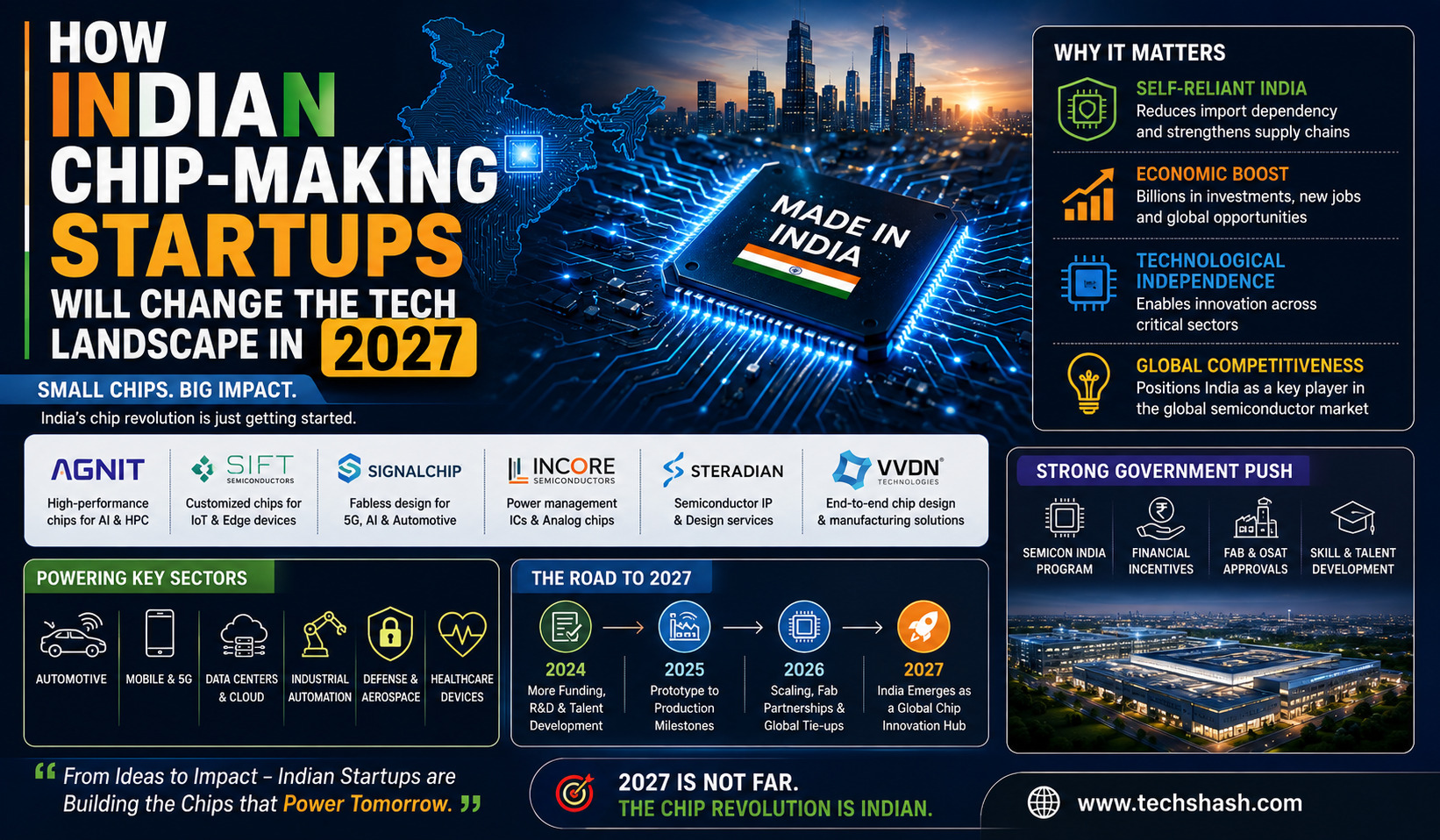
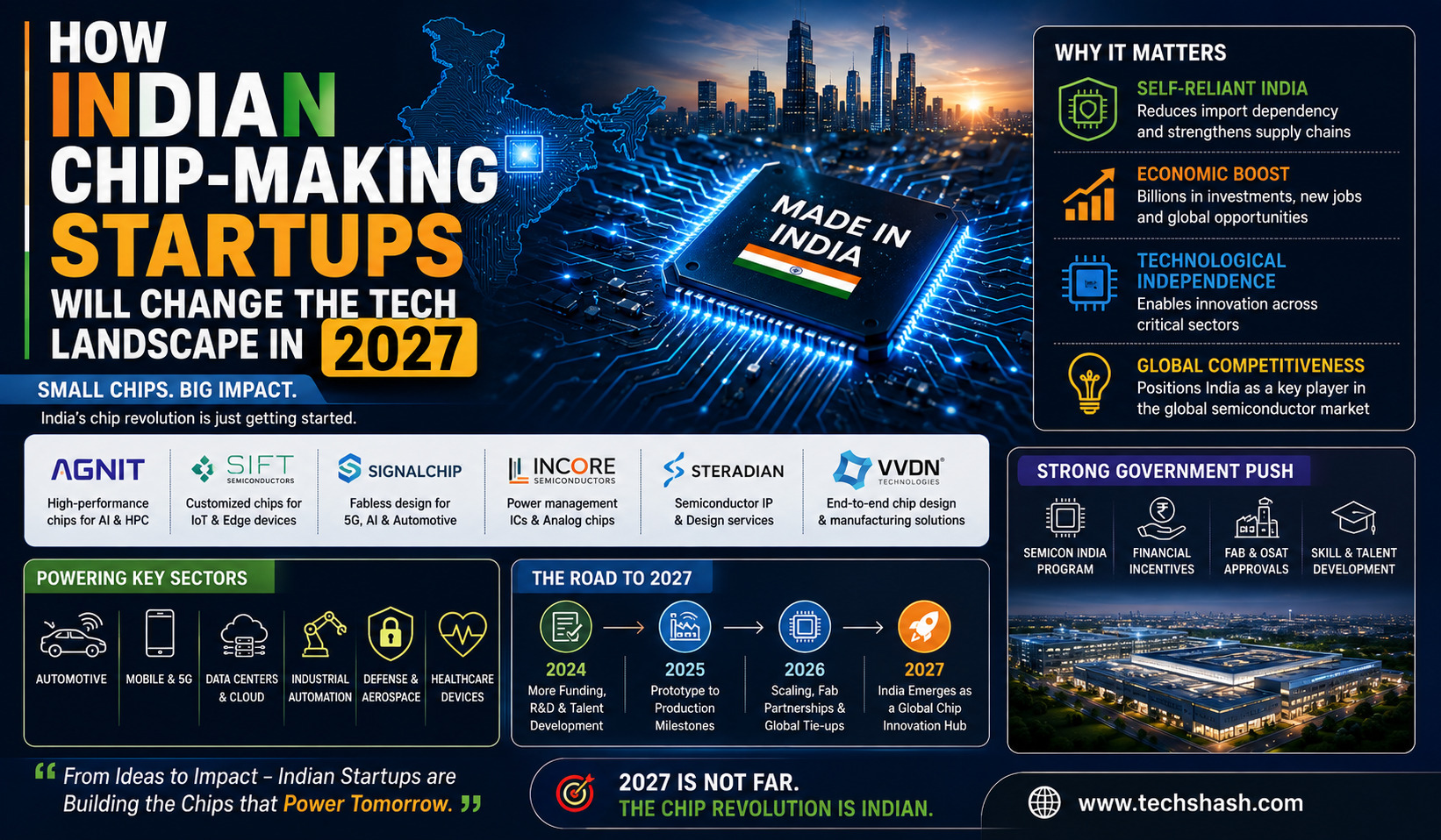
India’s chip design startups have quietly moved from side projects to a funded, government-backed industry. As the country heads toward 2027, a wave of fabless companies is turning years of design outsourcing experience into homegrown products. This article covers what has already happened, what funding and policy changes are driving it, and what to watch as more of these startups mature.
Where India’s Chip Startup Scene Stands Today
India built its semiconductor reputation on design services, not chip ownership. Design centers across the country employ a large engineering workforce and have historically designed chips for foreign clients rather than for themselves. That pattern is shifting. Companies such as Saankhya Labs and newer entrants like C2i now design and sell their own chips, aiming at sectors including AI, IoT, telecom, and defense.
Most of these startups cluster in Bengaluru, Hyderabad, and Chennai, the country’s established chip design hubs. Many are betting on open-source RISC-V processors, 5G system-on-chip designs, edge AI accelerators, and energy-efficient power management chips rather than trying to compete head-on in cutting-edge logic chips.
The Government Support Fueling These Startups
The Design Linked Incentive (DLI) scheme, run under the India Semiconductor Mission, sits behind much of this growth. It reimburses up to 50 percent of eligible design costs and gives startups access to expensive electronic design automation tools and shared infrastructure they could not otherwise afford.
By early 2026, the Ministry of Electronics and Information Technology had approved 23 design projects and extended infrastructure support to more than 70 firms. A related effort, the Chips to Startup program, has given over 67,000 engineering students across more than 100 universities direct access to industry-grade EDA software, building the talent pipeline these startups will draw from for years to come.
Funding Growth and Tape-Out Milestones
The funding numbers tell their own story. Startup investment in India’s semiconductor sector grew from about $5 million in 2023 to roughly $50 million in 2025, a tenfold jump in two years. Separately, DLI-backed startups alone have raised more than ₹430 crore, close to $45 million, from venture investors.
Design work is also turning into finished silicon. Indian startups have completed 16 successful tape-outs, the point where a chip design is finalized and sent for manufacturing, including designs built on advanced 12-nanometer process nodes. That is a meaningful shift from a design-only economy toward one producing real, manufactured products.
Names Worth Knowing in This Space
A handful of companies illustrate the range of what is happening:
- Saankhya Labs: An established player often cited as a pioneer of India’s fabless chip movement.
- C2i: A newer entrant representing the current wave of DLI-backed startups.
- Cirel Systems and Steradian Semi: Startups that have competed against established global players in their respective niches.
Together, these companies span both older, more established firms and a newer generation moving through the DLI pipeline, reflecting a broader base than any single flagship company can represent on its own.
What Semicon 2.0 Changes Going Into 2027
India’s semiconductor policy is entering a second phase, referred to as Semicon 2.0, approved by the Union Cabinet in July 2026 with a total outlay of ₹1,27,500 crore, close to $13.33 billion. For fabless startups specifically, this phase removes prior funding caps, allowing support to potentially reach ₹1,000 crore, around $104.6 million, per project.
That change matters heading into 2027 because it addresses a structural gap in the earlier support system. Indian fabless companies have historically had strong design capability but limited paths to actually get their chips manufactured at scale, since India lacked its own foundry capacity until recently. Semicon 2.0’s larger per-project support is aimed squarely at closing that gap.
How This Connects to India’s Fabrication Push
Chip design startups do not operate in isolation from India’s manufacturing buildout. The Tata-PSMC fab in Dholera, Gujarat, is targeting its first wafer output in December 2026, positioned as India’s first commercial 28-nanometer fabrication facility, with a reported investment of around ₹91,000 crore, close to $10.9 billion. Once operational, facilities like this could give Indian-designed chips a path to local manufacturing rather than relying entirely on foreign foundries.
Assembly and packaging capacity is also coming online alongside design growth. The Micron ATMP facility in Sanand, Gujarat, was inaugurated by Prime Minister Modi on February 28, 2026, marking India’s first global semiconductor assembly and test facility. CG Power has also launched an OSAT pilot line in Sanand, with its initial G1 facility handling around 0.5 million units per day and a planned G2 line expected to scale to 14.5 million units per day.
Analysts tracking the sector estimate India’s semiconductor market grew from around $38 billion in 2023 to an estimated $45 to $50 billion in 2025, with projections putting it above $100 billion by 2030. Whether that growth materializes depends heavily on whether design startups and fabrication capacity scale together rather than in isolation.
Global Foundries Are Starting to Notice
The shift toward homegrown chip products has also caught the attention of foreign foundries. Indian companies that spent the last decade providing design services to overseas semiconductor firms now need ongoing wafer production for their own chips, not one-time design contracts. That change in demand is drawing attention from foundries abroad.
South Korean foundry DB HiTek, for example, is attending electronica India 2026 for the first time as part of its India strategy. The trade show itself expanded in 2026 to two annual editions, with a North India edition in Greater Noida drawing 355 exhibitors from 19 countries in April, and a South India edition planned for Bengaluru in September, reflecting how much international interest the design startup boom has generated.
Key Takeaways
- Shift from services to products: Indian design firms are increasingly building and selling their own chips instead of only serving foreign clients.
- Government-backed funding: The DLI scheme has funded more than 20 startups and helped attract close to ₹430 crore in venture capital.
- Real output, not just design: Sixteen tape-outs, including 12-nanometer designs, show design work converting into manufactured silicon.
- Bigger support coming: Semicon 2.0 removes prior funding caps, raising potential per-project support to about $104.6 million.
- Manufacturing catching up: The Tata-PSMC fab in Dholera targets first wafer output by December 2026, a milestone that could support local chip production for these startups.
- Market growth projected: Analysts expect India’s semiconductor market to exceed $100 billion by 2030, up from an estimated $45 to $50 billion in 2025.
- Foreign foundries taking notice: South Korean foundry DB HiTek is attending an Indian trade show for the first time, a sign of growing international interest in local wafer demand.
Frequently Asked Questions
What is the Design Linked Incentive scheme?
It is a government program that reimburses up to 50 percent of eligible chip design costs and provides access to design tools and infrastructure for fabless startups.
How many chip design startups has India supported so far?
By early 2026, the government had approved 23 design projects and supported more than 70 firms with infrastructure access.
What is Semicon 2.0?
Semicon 2.0 is the second phase of the India Semiconductor Mission, approved in July 2026 with a total outlay of about $13.33 billion, and it removes previous funding caps for fabless startups.
Which Indian chip startups are considered leaders in this space?
Saankhya Labs is often cited as an established pioneer, alongside newer entrants like C2i, Cirel Systems, and Steradian Semi.
Will India’s chip startups have access to local manufacturing by 2027?
The Tata-PSMC fab in Dholera is targeting first wafer output by December 2026, which could give local chip designers a path to domestic manufacturing going into 2027.
Are foreign foundries interested in India’s chip design boom?
Yes, foundries such as South Korea’s DB HiTek are actively pursuing India as a market, drawn by rising wafer demand from local fabless companies.
Conclusion
India’s chip-making startups are heading into 2027 with more government funding, more finished tape-outs, and a policy shift under Semicon 2.0 that removes some of the earlier limits on support. None of this guarantees a dramatic transformation on its own, but the combination of design talent, funding growth, and approaching local fabrication capacity gives these startups a genuinely different starting position than they had just a few years ago.